


 It’s Only Common Sense: OCCAM—the Time Is Now
 Marcy's Musings: The Growing Industry
 Dan’s Biz Bookshelf: Seeing the How
Megasonic Acoustic Surface Treatment Process for Enhanced Copper Electrodeposition in Via Interconnects
July 4, 2017 | Thomas Jones, Dr. David Flynn, Marc P.Y. Desmulliez and Dennis PriceEstimated reading time: 1 minute
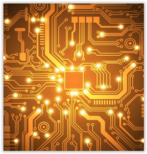
Introduction
A printed circuit board is populated with a multitude of electro-mechanical components plus various active and passive devices such as transistors, capacitors, inductors and resistors, which enable the functionality and assembly of the PCB. Increasing the density of the components on the surface of a board enables greater functionality and use. A high-density (HD) design is desirable for technology high end applications, which include automotive, aerospace, space, defense, mobile phones, medical, networking, communications, and computer storage[1].
The current trend in PCB markets is lowtechnology, high-volume demand and is typically supplied by low-cost, large-scale facilities in Southeast Asia, such as China, India and Thailand. High-value, low-volume PCB markets are typically supplied by smaller-sized facilities in western regions such as North America and Europe, but also economically developed east
ern locations such as Japan, South Korea and Taiwan[2]. The UK PCB demand typically focuses on this latter market. Manufacturing developments bringing increased capability and cost savings to a factory in the UK would be highly desirable and enable increased market competitiveness. For more than four years, Merlin Circuit Technology Ltd (MCT), in Deeside, North Wales, has been working in collaboration with Heriot-Watt University (HWU) in Edinburgh, Scotland, on a UK government project funded by the Engineering and Physical Sciences Research Council (EPSRC), looking to improve HD PCB manufacturing capability through enhancements to the electrodeposition of copper using high frequency acoustic, applied within a copper plating bath [3,4,5]. This article outlines some of the key findings from this project.
To read the full version of this article which appeared in the June 2017 issue of The PCB Magazine.
Share on:


Suggested Items
Designer’s Notebook: What Designers Need to Know About Manufacturing, Part 2
04/24/2024 | Vern Solberg -- Column: Designer's NotebookThe printed circuit board (PCB) is the primary base element for providing the interconnect platform for mounting and electrically joining electronic components. When assessing PCB design complexity, first consider the component area and board area ratio. If the surface area for the component interface is restricted, it may justify adopting multilayer or multilayer sequential buildup (SBU) PCB fabrication to enable a more efficient sub-surface circuit interconnect.
Insulectro’s 'Storekeepers' Extend Their Welcome to Technology Village at IPC APEX EXPO
04/03/2024 | InsulectroInsulectro, the largest distributor of materials for use in the manufacture of PCBs and printed electronics, welcomes attendees to its TECHNOLOGY VILLAGE during this year’s IPC APEX EXPO at the Anaheim Convention Center, April 9-11, 2024.
ENNOVI Introduces a New Flexible Circuit Production Process for Low Voltage Connectivity in EV Battery Cell Contacting Systems
04/03/2024 | PRNewswireENNOVI, a mobility electrification solutions partner, introduces a more advanced and sustainable way of producing flexible circuits for low voltage signals in electric vehicle (EV) battery cell contacting systems.
Heavy Copper PCBs: Bridging the Gap Between Design and Fabrication, Part 1
04/01/2024 | Yash Sutariya, Saturn Electronics ServicesThey call me Sparky. This is due to my talent for getting shocked by a variety of voltages and because I cannot seem to keep my hands out of power control cabinets. While I do not have the time to throw the knife switch to the off position, that doesn’t stop me from sticking screwdrivers into the fuse boxes. In all honesty, I’m lucky to be alive. Fortunately, I also have a talent for building high-voltage heavy copper circuit boards. Since this is where I spend most of my time, I can guide you through some potential design for manufacturability (DFM) hazards you may encounter with heavy copper design.
Trouble in Your Tank: Supporting IC Substrates and Advanced Packaging, Part 5
03/19/2024 | Michael Carano -- Column: Trouble in Your TankDirect metallization systems based on conductive graphite or carbon dispersion are quickly gaining acceptance worldwide. Indeed, the environmental and productivity gains one can achieve with these processes are outstanding. In today’s highly competitive and litigious environment, direct metallization reduces costs associated with compliance, waste treatment, and legal issues related to chemical exposure. What makes these processes leaders in the direct metallization space?