-

- News
- Books
Featured Books
- pcb007 Magazine
Latest Issues
Current Issue
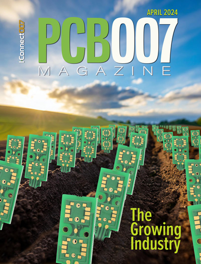
The Growing Industry
In this issue of PCB007 Magazine, we talk with leading economic experts, advocacy specialists in Washington, D.C., and PCB company leadership to get a well-rounded picture of what’s happening in the industry today. Don’t miss it.

The Sustainability Issue
Sustainability is one of the most widely used terms in business today, especially for electronics and manufacturing but what does it mean to you? We explore the environmental, business, and economic impacts.

The Fabricator’s Guide to IPC APEX EXPO
This issue previews many of the important events taking place at this year's show and highlights some changes and opportunities. So, buckle up. We are counting down to IPC APEX EXPO 2024.
- Articles
- Columns
Search Console
- Links
- Events
||| MENU - pcb007 Magazine
The Impact of Chip Packaging
February 1, 2023 | Charles E. Bauer, Ph.D., TechLead CorporationEstimated reading time: 1 minute
When talking about chip packaging impacts on substrates and electronic manufacturing services (EMS) providers, the focus mostly lies on large packages and very high I/O, fine pitch components; rightly so in most cases. However, several current packaging trends offer a new path forward to simplification and, thereby, cost reduction in both the printed wiring board (PWB) and EMS supply chains.
A handful of key technologies support these advances. Through silicon vias (TSV), while tracing their origins back to the invention of the transistor and found in a few supercomputers during the 1980s, really came onto the volume manufacturing scene between 2005 and 2010. Since that time, rapid advances in process control and yield led to very high-density memory implementations. TSV now proves a key enabler in the evolution of chiplet architectures.
The second key technology development came in the form of silicon and glass substrate development. Silicon substrates entered the scene in a significant manner during the 1990s but, until recently, proved too expensive for all but the most esoteric applications. The availability of old node fabrication equipment that flooded the market around 2008–10, opened the door to more reasonably priced Si substrate and provided an easy path to the current chiplet architecture, particularly for large IC OEMs. The advent of glass substrates, driven by extensive research at the Georgia Tech Packaging Research Center, now provides very high routing capability comparable with silicon substrates at far lower cost. The compatibility between the coefficient of thermal expansion (CTE) of glass and Si chips makes for highly reliable, multichip assembly either in a chiplet or SiP application.
To read this entire article, which appeared in the January 2023 issue of PCB007 Magazine, click here.
Suggested Items
Ark Electronics Expands Global Manufacturing Factory Network in North America and Europe
04/17/2024 | PRNewswireElectronic Manufacturing Company Ark Electronics recently announced the expansion of its Global Factory Network with the addition of Electronics Manufacturing Service (EMS) capabilities in Mexico and Europe.
Microchip Technology Acquires Neuronix AI Labs
04/16/2024 | Microchip Technology Inc.Innovative technology enhances AI-enabled intelligent edge solutions and increases neural networking capabilities.
Fluor Awarded U.S. Air Force Contract Augmentation Program V Task Order for Tinian
04/11/2024 | BUSINESS WIREFluor Corporation announced that the U.S. Air Force Installation Contracting Agency awarded the company a task order contract for Pavement and Transportation Support North Field, Tinian, Commonwealth of the Northern Mariana Islands (CNMI).
ENNOVI Introduces a New Flexible Circuit Production Process for Low Voltage Connectivity in EV Battery Cell Contacting Systems
04/03/2024 | PRNewswireENNOVI, a mobility electrification solutions partner, introduces a more advanced and sustainable way of producing flexible circuits for low voltage signals in electric vehicle (EV) battery cell contacting systems.
Intel Outlines Financial Framework for Foundry Business, Sets Path to Margin Expansion
04/03/2024 | BUSINESS WIREIntel Corporation outlined a new financial reporting structure that is aligned with the company’s previously announced foundry operating model for 2024 and beyond.


