


 Material Insight: The Dielectric Constant of PCB Materials
 American Made Advocacy: What About the Rest of the Technology Stack?
 It’s Only Common Sense: Great Ideas From John Mitchell’s Book on Hiring Habits
An Examination of Glass-fiber and Epoxy Interface Degradation in Printed Circuit Boards
July 12, 2019 | Bhanu Sood, Michael Osterman, and Michael Pecht, Center for Advanced Life Cycle EngineeringEstimated reading time: 9 minutes
Multilayer organic laminates, which make up over 90% of the interconnecting substrates in electronics (standard FR-4 represents 85% of the substrates used for laminates), can develop a loss of electrical insulation resistance between two biased conductors due to conductive filament formation. The probability of conductive filament formation is a function of the temperature, moisture content, voltage bias, manufacturing quality and processes, materials, and other environmental conditions and physical factors.
With increases in design density and tighter spacing between conductors, the probability of failure due to conductive filament formation (CFF) in printed circuit board (PCB) electronic assemblies has increased. CFF is a failure observed within glass-reinforced epoxy PCB laminates caused by an electrochemical process involving the ionic transport of a metal through or across a non-metallic medium under the influence of an applied electric field [1 & 2]. The growth of the metallic filament is a function of temperature, humidity, voltage, laminate materials, manufacturing processes, and the geometry and spacing of the conductors [2]. The growth of these filaments can cause an abrupt loss of insulation resistance between the conductors under a DC voltage bias.
A statistical examination of field returns and root cause analysis performed at the Center for Advanced Life Cycle Engineering (CALCE) at the University of Maryland shows that failures in PCBs account for a significant percentage of field returns in electronic products and systems. Studies on CFF [2 & 3] have found that path formation in a PCB is often along the glass fiber to epoxy matrix interface (Figure 1).
Figure 1: Schematic describing CFF growth [3].
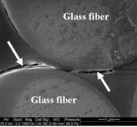
Delamination along the fiber-resin interface can occur as a result of stresses generated under thermal cycling due to coefficient of thermal expansion (CTE) mismatch between the glass fiber (CTE = ~5.5 ppm/°C) and the epoxy resin (CTE = ~65 ppm/°C) (Figure 2). CFF can take place in the plated through-hole to plated through-hole (PTH-PTH), PTH-plane, and trace-trace geometries.
Figure 2: CFF growth path along the glass fiber and resin interface [3].
A two-step model was developed to explain the growth of conductive filaments at the resin-glass interface in PCBs [1 & 3] where degradation of the resin-glass interfacial bond first occurs, followed by an electrochemical reaction. According to Lando [2], the path required for the transportation of metal ions formed by the degradation of the resin-glass interfacial bond results from the mechanical release of stresses, poor glass treatment, hydrolysis of the silane glass finish, or stresses originating from moisture-induced swelling of the epoxy resin.
Path formation was reported to be independent of bias; however, humidity was identified as a contributing factor towards degradation. After path formation, the PCB is viewed as an electrochemical cell. In this cell, the copper conductors are the electrodes, the absorbed water is the electrolyte, and the driving potential for the electrochemistry is the operating or test potential of the circuit. The electrode reactions for the metal migration are:
At the anode:
Equation 1:
Equation 2:
At the cathode:
Equation 3:
Pathway Formation in CFF
In PCBs, one manner in which the pathway between conductors is formed is through chemical hydrolysis of the silane glass finish or coupling agent. Past work has shown that the glass epoxy interface absorbs five to seven times more moisture than the bulk epoxy [5]. A common cross-linking agent used in FR-4 and many other epoxy-based laminated systems is dicyandiamide, or dicy. Dicy and glass surfaces are both hydrophilic. This combination of a hydrophilic surface and cross-linking agent is one of the factors responsible for the degradation of the glass fiber-epoxy resin interface due to hydrolysis. Williams [6] has shown that PCBs manufactured with non-dicy cross-linked epoxy resins are more resistance to CFF failures than PCBs manufactured with dicy cross-linked epoxy resins.
Organosilanes are bifunctional molecules that act as adhesion promoters, crosslink agents, and moisture scavengers in adhesive and sealant products [7]. Silane adhesion promoters act as molecular bridges between two chemically different materials and have been shown to dramatically improve the adhesion of polymeric resins to substrates such as glass, silica, alumina, or active metals.
Page 1 of 3
Share on:


Suggested Items
DuPont Showcases AI Innovations Featuring Advanced Interconnects at 2024 International Electronic Circuits Exhibition
05/13/2024 | DuPontDuPont announced it will showcase its comprehensive range of advanced circuit materials and solutions at the 2024 International Electronic Circuits Exhibition in Shanghai. With a product portfolio that includes fine line, signal integrity, power and thermal management, DuPont will exhibit at Booth #8L06 at the National Exhibition and Convention Center (NECC) from May 13 to 15.
MKS’ Atotech to Participate in ECTC
05/10/2024 | MKS’ AtotechAt this year’s 74th IEEE Electronic Components and Technology Conference (ECTC), MKS’ Atotech will present and demonstrate its latest product and service innovations.
The Chemical Connection: Reducing Etch System Water Usage, Part 2
05/02/2024 | Don Ball -- Column: The Chemical ConnectionIn my last column, I reviewed some relatively simple ways to reduce water usage in existing etch systems: cutting down cooling coil water flow, adding chillers to replace plant water for cooling, lowering flow rate nozzles for rinses, etc. This month, I’ll continue with more ways to control water usage in your etcher. Most of these are not easily retrofittable to existing equipment but should be given serious consideration when new equipment is contemplated. With the right combination of add-ons, it is possible to bring the amount of water used in an etch system to almost zero.
Designer’s Notebook: What Designers Need to Know About Manufacturing, Part 2
04/24/2024 | Vern Solberg -- Column: Designer's NotebookThe printed circuit board (PCB) is the primary base element for providing the interconnect platform for mounting and electrically joining electronic components. When assessing PCB design complexity, first consider the component area and board area ratio. If the surface area for the component interface is restricted, it may justify adopting multilayer or multilayer sequential buildup (SBU) PCB fabrication to enable a more efficient sub-surface circuit interconnect.
Insulectro’s 'Storekeepers' Extend Their Welcome to Technology Village at IPC APEX EXPO
04/03/2024 | InsulectroInsulectro, the largest distributor of materials for use in the manufacture of PCBs and printed electronics, welcomes attendees to its TECHNOLOGY VILLAGE during this year’s IPC APEX EXPO at the Anaheim Convention Center, April 9-11, 2024.