


 Material Insight: The Dielectric Constant of PCB Materials
 American Made Advocacy: What About the Rest of the Technology Stack?
 It’s Only Common Sense: Great Ideas From John Mitchell’s Book on Hiring Habits
Not All Plating Lines Are Created Equal
February 12, 2020 | I-Connect007 Editorial TeamEstimated reading time: 12 minutes
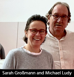
Barry Matties and Happy Holden met with CEO Michael Ludy and CMO Sarah Großmann from Ludy, a company specializing in galvanic plating equipment for PCBs. During one of I-Connect007’s visit to GreenSource Fabrication, the team found Ludy equipment being utilized there, so Barry and Happy traveled to their factory in Germany to learn more about the company.
The following interview gives an overview of Ludy and their latest advancements in PCB plating equipment.
Barry Matties: Let’s start with a little bit about your product.
Sarah Großmann: We produce galvanic plants for PCBs. That’s our main task. We have a highly specialized way of having the galvanic tanks and the geometry of the tanks, where the plating and the aspect ratio is much better. We tried to focus mainly on PCBs in the past years. We fulfilled the demands and ideas of Alex Stepinski and what he thought could work. We are flexible and gave him a plant with the newest technology. He can fulfill his plating demands and multiple processes internally.
Generally, this is the main thing we do, but we also do the research for waste-air-free and wastewater-free galvanic plants like the GalvanoMat® PCB. That’s our main idea of fulfilling a complete green fabrication in one. You have one container where the galvanic plant is inside, and one container getting the waste air, wastewater, and energy recovery, and everything goes in one circle. You don’t have to waste that much and fulfill all the green fabrication requirements that are needed.
We have it for metal finishing and PCBs. We’re trying to get back in the U.S. market. We were there already. The lines are still running, and it’s going more and more to green fabrication. This is why we mostly do R&D for the GalvanoMat® PCB.
Figure 1: Overview of the latest generation of Ludy plating line with split-tank hoist access.
Happy Holden: People would probably buy brand new plating equipment because of high-density interconnect (HDI) and substrate-like PCBs (SLPs). All of which have very tiny holes and a much higher aspect ratio, which the conventional anode to cathode and one-axis agitation or area agitation is not sufficient for the throwing power and things like that.
Großmann: The anodes are inside, and every one of those segmented anodes is separately controlled by a rectifier.
Holden: Can you do pulse plating too?
Großmann: It would be possible, depending on the chemistry. The problem is that in the galvanic plant area, the people stick to what they know and don’t want to invest high amounts of money for testing around. This is a problem. That’s why the research steps are not very fast compared to other machine areas. They know that the chemistry is also influencing this area, and if Atotech says they’re not sure, then nobody will invest money on that. That’s why we are pretty happy that our solution worked and was inclusive with a 3D agitation drive. We have a very good distribution overall of the PCB on both sides. Those are the main benefits of the system.
Holden: The North American market has the common board, but then they have leading-edge things for medical, aerospace, or radar, where they want to go to a much higher aspect ratio both on through-holes and on blind vias. The problem is typical galvanic equipment isn’t there yet. Some believe the Ludy equipment will take them there, which means adopting the old way. There’s a big difference in productivity between four hours and 50 minutes.Page 1 of 4
Share on:


Suggested Items
DuPont Showcases AI Innovations Featuring Advanced Interconnects at 2024 International Electronic Circuits Exhibition
05/13/2024 | DuPontDuPont announced it will showcase its comprehensive range of advanced circuit materials and solutions at the 2024 International Electronic Circuits Exhibition in Shanghai. With a product portfolio that includes fine line, signal integrity, power and thermal management, DuPont will exhibit at Booth #8L06 at the National Exhibition and Convention Center (NECC) from May 13 to 15.
MKS’ Atotech to Participate in ECTC
05/10/2024 | MKS’ AtotechAt this year’s 74th IEEE Electronic Components and Technology Conference (ECTC), MKS’ Atotech will present and demonstrate its latest product and service innovations.
The Chemical Connection: Reducing Etch System Water Usage, Part 2
05/02/2024 | Don Ball -- Column: The Chemical ConnectionIn my last column, I reviewed some relatively simple ways to reduce water usage in existing etch systems: cutting down cooling coil water flow, adding chillers to replace plant water for cooling, lowering flow rate nozzles for rinses, etc. This month, I’ll continue with more ways to control water usage in your etcher. Most of these are not easily retrofittable to existing equipment but should be given serious consideration when new equipment is contemplated. With the right combination of add-ons, it is possible to bring the amount of water used in an etch system to almost zero.
Designer’s Notebook: What Designers Need to Know About Manufacturing, Part 2
04/24/2024 | Vern Solberg -- Column: Designer's NotebookThe printed circuit board (PCB) is the primary base element for providing the interconnect platform for mounting and electrically joining electronic components. When assessing PCB design complexity, first consider the component area and board area ratio. If the surface area for the component interface is restricted, it may justify adopting multilayer or multilayer sequential buildup (SBU) PCB fabrication to enable a more efficient sub-surface circuit interconnect.
Insulectro’s 'Storekeepers' Extend Their Welcome to Technology Village at IPC APEX EXPO
04/03/2024 | InsulectroInsulectro, the largest distributor of materials for use in the manufacture of PCBs and printed electronics, welcomes attendees to its TECHNOLOGY VILLAGE during this year’s IPC APEX EXPO at the Anaheim Convention Center, April 9-11, 2024.